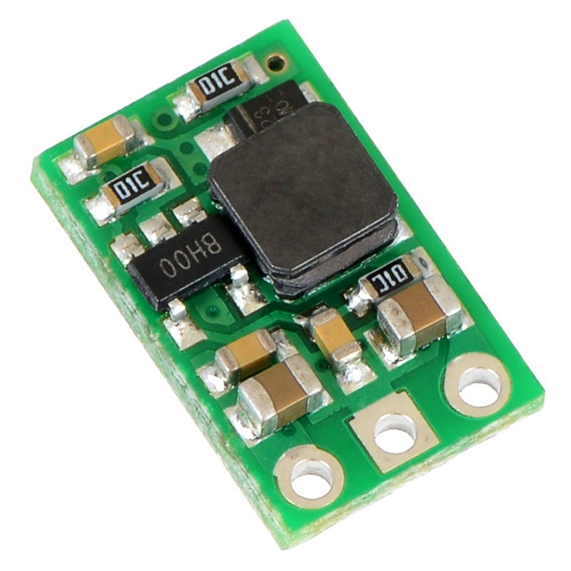

Pololu 12V Step-Up Voltage Regulator U3V12F12
Pololu 12V Step-Up Voltage Regulator U3V12F12
In stock
Couldn't load pickup availability
Overview
These boost (step-up) voltage regulators generate higher output
voltages from input voltages as low as 2.5 V. They are switching
regulators (also called switched-mode power supplies (SMPS) or DC-to-DC
converters) and have a typical efficiency between 80% to 90%. The
available output current is a function of the input voltage, output
voltage, and efficiency (see Typical Efficiency and Output Current
section below), but the input current can typically be as high as
1.4 A. This regulator is available with a fixed 5 V, 9 V, or 12 V
output:
Select options:
The regulator’s thermal shutdown prevents damage from overheating, but it does not have short-circuit or reverse-voltage protection.


 |
Features
- input voltage: 2.5 V – VOUT
- fixed 5 V, 9 V, or 12 V output with 4% accuracy
- 1.4 A switch allows for input currents up to 1.4 A
- 2 mA typical no-load quiescent current
- integrated over-temperature shutoff
- small size: 0.515″ × 0.32″ × 0.1″ (13 × 8 × 3 mm)
Using the Regulator
Connections
The boost regulator has three connections: input voltage (VIN), ground (GND), and output voltage (VOUT).
The input voltage, VIN, must be at least 2.5 V and should not exceed
the output voltage, VOUT. Please be wary of destructive LC spikes that
might cause the input voltage to exceed VOUT (see below for more
information).
The three connections are labeled on the back side of the PCB, and
they are arranged with a 0.1″ spacing along the edge of the board for
compatibility with solderless breadboards, connectors,
and other prototyping arrangements that use a 0.1″ grid. You can
solder wires directly to the board or solder in either the 3×1 straight male header strip or the 3×1 right-angle male header strip that is included.
 |
Typical Efficiency and Output Current
The efficiency of a voltage regulator, defined as
(Power out)/(Power in), is an important measure of its performance,
especially when battery life or heat are concerns. As shown in the
graphs below, this switching regulator typically has an efficiency of 80
to 90%.
 |
 |
 |
The maximum achievable output current is approximately
proportional to the ratio of the input voltage to the output voltage.
If the input current exceeds the switch current limit
(typically somewhere between 1.4 and 2 A), the output voltage will begin
to drop. Additionally, the maximum output current can depend on other
factors, including the ambient temperature, air flow, and heat sinking.
LC Voltage Spikes
When connecting voltage to electronic circuits, the initial rush of
current can cause damaging voltage spikes that are much higher than the
input voltage. In our tests with typical power leads (~30″ test clips),
input voltages above 10 V caused voltage spikes in excess of 20 V. You
can suppress such spikes by soldering a 33μF or larger electrolytic
capacitor close to the regulator between VIN and GND.